

The Internet of Things (IoT), radio-frequency identification (RFID) and sensors are hot topics these days. A new age is unraveling in which various everyday things are connected to sensors and the internet.
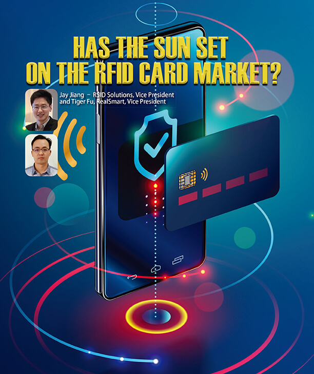
RFID, which was invented decades ago, has been in use since World War II. RFID pertains to the use of radio waves to read and capture information stored on a tag attached to an object. The technology has evolved in the past 20 years and today is mainly used for contactless cards.
RFID card usage has matured in European and Asian countries and continues to grow throughout the world with 1 billion shipped annually. However, given the recent introduction of various e-payment, e-ID and bio-recognition technologies, are there any opportunities left for RFID in the card industry? The answer is yes.
The rapid production of RFID cards has put enormous demands on the sheet inlay and other card manufacturing support industries. Today’s market is calling for pre-laminated inlays.
In Japan, the Suica transportation card is flatter and has superior surface finishing when compared to other cards. A pre-laminated inlay is the key technology used to accomplish these card characteristics.
Few card manufacturers can make 125 KHz RFID proximity cards flat enough for ideal printing. When designing the printed area of these cards, the chip and antenna location have to be avoided.
Another challenge for the card industry is reducing inlay thickness. The International Standards Organization (ISO) has set a card thickness limitation of .84 mm. When applying additional foil or another functional material layer for an anti-counterfeiting application, it’s hard to make pre-laminates under .30 mm.
To find a solution to these issues, let’s analyze the common structure of a card inlay.
The four-layer formula, which is mainly used for high frequency (HF) 13.56 MHz inlay production for banking and MIFARE cards, means one small and one large hole are punched into the card before the chip is inserted.
After laminating the chip area, the inlay surface is not flat due to defective melting and cooling and shrinkage in the chip and surrounding areas. In general, such pre-laminated inlays measure 380-420 microns and it is difficult to make them thinner due to current chip encapsulation technology.
The three-layer formula is also commonly used for HF card inlay production. A hole is punched in the middle of the plastic layer for chip insertion before collating the top and bottom plastic layers together for lamination. This allows for the hot-melted material to fill in the gaps between the plastic and the chip encapsulation. After laminating the chip area, the inlay surface is not flat due to defective melting and cooling shrinkage in the chip and surrounding areas. In general, such pre-laminated inlays measure 380-420 microns and it is difficult to make them thinner due to current chip encapsulation technology.
The two-layer formula is popular for 125 KHz card inlay production. The transponder is placed on the bottom plastic layer, which is collated to the top layer for lamination. The gap between the transponder and plastic will be filled by the heated material, but the inlay surface will not be flat due to cooling shrinkage during the lamination process.
Most manufacturers can’t find a cost-effective way to produce high-quality, flat low-frequency (LF) pre-laminates. Due to thickness limitations on LF coils and chip encapsulation, pre-laminate inlays are typically 500-550 microns. With such inlays, it’s not difficult to end up with a card thickness of 800 microns or more than 840 microns. And there’s no way to apply an anti-counterfeiting layer or other application materials.
There’s another way of applying etching-aluminum or copper-etched antenna—with flip-chip bonding (dry inlay) in the middle layer. Put the dry inlay layer between the top and bottom plastic layers and then laminate them together. This technology produces pre-laminated inlays that measure 330-350 microns. However, the antenna is on polyester (PET) film, which is hard to glue to the top and bottom plastic layers due to different properties of the materials. This also produces a ripple effect on a glossy card finish. Aluminum on PET film will cause defects after card lamination.
Now, let’s consider the RFID chip and encapsulation. Making thinner chip encapsulations would reduce LF or HF card thickness. However, no one in the industry has been able to make chip packaging with a thickness less than 200 microns.
Another way to reduce card thickness would be to manufacture inlays with materials other than PVC, such as PET, PETG, polycarbonate or Teslin.
When it comes to pre-laminated inlay trends in the near future, we may see:
Super-thin:
If manufacturers could create pre-laminate inlays that measure less than 200 microns, there would be room to add features such as anti-forgery film or laser-engravable polycarbonate.
Directly printable:
There
is a market demand for flat and thin plastic sheets that can be printed on
directly with offset or digital printing.
Ultra-flat:
Pre-laminate inlays must be flat for printing to give the card a quality appearance. This would also overcome the current ID card printing challenges.
Test prior to punch:

The current methods of pre-laminate inlay testing are manual reading, semi-automatic and fully automatic. Manual reading is a primitive means of testing that requires handling a reader with an alarm. Sometimes, microcracks in chips cannot be detected, which leads to personalization and use problems. The semi-automatic testing method means manually putting the sheet inlay onto the platform of a testing machine that will automatically scan and recognize defective transponders. The fully automatic method means testing the inlay/transponder after soldering or pre-laminating the inlay on an auto-inlay testing machine. This means having the ability to encode chips for initialization, change keys or write specific data.
Future testing methods could utilize the cloud platform to upload relevant data during production and testing. Companies could use the data as they wish. Future testing methods should also include intelligent production and automation, which means with the click of a mouse all testing and production tasks could easily be done with an automated system.
The recent introduction of a pre-laminated inlay with a minimum thickness of 200 microns and unparalleled super-thin and ultra-flat features means the future of card manufacturing has arrived. Regardless of the chip, layout or materials used or whether the card is printed directly or made into an ID card with super finish, this inlay overcomes the challenges of ideal printing and creates opportunities for those who want to print freely with great results. ID card and security document manufacturers have more space to apply more functional materials. The newly-introduced inlay can also be used for ID card printer applications and it supports PVC, polycarbonate and Teslin.
While the first generation of these inlays are currently being shipped to millions of customers, an optimized version is currently in the works that should be more attractive to card industry players who aim to stay ahead of their competition.